Nvidia Taps Memory, Switch for AI

发布时间:2018-03-28 00:00
作者:Ameya360
来源:Rick Merritt
阅读量:3391

  At its annual GTC event, Nvidia announced system-level enhancements to boost the performance of its GPUs in training neural networks and a partnership with ARM to spread its technology into inference jobs.

  Nvidia offered no details of its roadmap, presumably for 7-nm graphics processors in 2019 or later. It has some breathing room, given that AMD is just getting started in this space, Intel is not expected to ship its Nervana accelerator until next year, and Graphcore — a leading startup — has gone quiet. A few months ago, both Intel and Graphcore were expected to release production silicon this year.

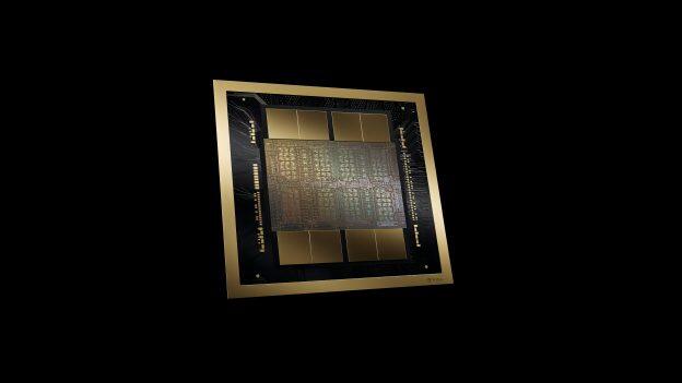
  The high-end Tesla V100 GPU from Nvidia is now available with 32-GBytes memory, twice the HBM2 stacks of DRAM that it supported when launched last May. In addition, the company announced NVSwitch, a 100-W chip made in a TSMC 12nm FinFET process. It sports 18 NVLink 2.0 ports that can link 16 GPUs to shared memory.

  Nvidia became the first company to make the muscular training systems expected to draw 10 kW of power and deliver up to 2 petaflops of performance. Its DGX-2 will pack 12 NVSwitch chips and 16 GPUs in a 10U chassis that can support two Intel Xeon hosts, Infiniband, or Ethernet networks and up to 60 solid-state drives.

  Cray, Hewlett Packard Enterprise, IBM, Lenovo, Supermicro, and Tyan said that they will start shipping systems with the 32-GB chips by June. Oracle plans to use the chip in a cloud service later in the year.

  Claims of performance increases using the memory, interconnect, and software optimizations ranged widely. Nvidia said that it trained a FAIRSeq translation model in two days, an eight-fold increase from a test in September using eight GPUs with 16-GBytes memory each. Separately, SAP said that it eked out a 10% gain in image recognition using a ResNet-152 model.

  Intel aims to leapfrog Nvidia next year with a production Nervana chip sporting 12 100-Gbit/s links compared to six 25-Gbit/s NVLinks on Nvidia’s Volta. The non-coherent memory of the Nervana chip will allow more flexibility in creating large clusters of accelerators, including torus networks, although it will be more difficult to program.

  To ease the coding job, Intel has released as open source its Ngraph compiler. It aims to turn software from third-party AI frameworks like Google’s TensorFlow into code that can run on Intel’s Xeon, Nervana, and eventually FPGA chips.

  The code, running on a prototype accelerator, is being fine-tuned by Intel and a handful of data center partners. The company aims to announce details of its plans at a developer conference in late May, though production chips are not expected until next year. At that point, Nvidia will be under pressure to field a next-generation part to keep pace with an Intel roadmap that calls for annual accelerator upgrades.

  ”The existing Nervana product will really be a software development vehicle. It was built on 28nm process before Intel bought the company and it's not competitive with Nvidia's 12nm Volta design,” said Kevin Krewell, a senior analyst with Tirias Research.

  Volta’s added memory and NVSwitch “keeps Nvidia ahead of the competition. We're all looking forward to the next process shrink, but, as far as production shipping silicon goes, Volta still has no peer,” he added.

  Among startups, Wave Computing is expected to ship this year its first training systems for data centers and developers. New players are still emerging.

  Startup SambaNova Systems debuted last week with $56 million from investors, including Google’s parent Alphabet. Co-founder Kunle Olukotun’s last startup, Afara Websystems, designed what became the Niagara server processor of Sun Microsystems, now Oracle.

  Nvidia currently dominates the training of neural network models in data centers, but it is a relative newcomer to the broader area of inference jobs at the edge of the network. To bolster its position, Nvidia and ARM agreed to collaborate on making Nvidia’s open-source hardware for inferencing available as part of ARM’s planned machine-learning products.

  Nvidia announced last year that it would open-source IP from its Xavier inference accelerator. It has made multiple RTL releases to date. The blocks compete with AI accelerators offered byCadence, Ceva, and Synopsys, among others.

  Just what Nvidia blocks that ARM will make available when remains unclear. So far, ARM has only sketched out its plans for AI chips as part of a broad Project Trillium. An ARM representative would only say that ARM aims to port its emerging neural net software to the Nvidia IP.

  Deepu Talla, general manager of Nvidia’s group overseeing Xavier, said that he is aware of multiple chips being designed using the free, modular IP. However, so far, none have been announced.

  Nvidia hopes that the inference effort spreads use of its machine-learning software also used in training AI models. To that end, the company announced several efforts to update its code and integrate it into third-party AI frameworks.

  TensorRT 4, the latest version of Nvidia’s runtime software, boosts support for inferencing jobs and is being integrated into version 1.7 of Google’s TensorFlow framework. Nvidia is also integrating the runtime with the Kaldi speech framework, Windows ML, and Matlab, among others.

  Separately, the company announced that the RTX software for ray tracing that it announced last week is now available on V100-based Quadro GV100 chips, sporting 32-GBytes memory and two NVLinks.

  The software enables faster, more realistic rendering for games, movies, and design models. It runs on Nvidia proprietary APIs as well as Microsoft’s DirectX for ray tracing and will support Vulkan in the future.

  The software delivers 10x to 100x improvements compared to CPU-based rendering that dominates a market that forecasts to be larger than $2 billion by 2020, said Bob Pette, vice president of Nvidia’s professional visualization group.

(备注:文章来源于网络,信息仅供参考,不代表本网站观点,如有侵权请联系删除!)

在线留言询价

相关阅读
NVIDIA Reportedly Halves Vera Rubin SOCAMM Capacity as Memory Costs Near 29% of System BOM
  Rising memory costs are prompting AI hardware vendors to rethink their product strategies. According to Wccftech, citing analysis from GF Securities, NVIDIA is reportedly reducing the memory capacity of its Vera Rubin NVL72 rack-scale AI system to cope with elevated memory prices and ongoing supply shortages. Without these adjustments, memory could account for around 29% of the Vera Rubin VR200 system’s estimated US$2.1 million bill of materials (BOM), well above NVIDIA’s preferred level of 20%.  The cost burden is significant. Wccftech, citing an earlier Bernstein report, notes that a single Vera Rubin NVL72 rack could cost as much as US$9.1 million, with memory accounting for a significant share of the cost. Bernstein also forecasts HBM4 pricing to rise to US$53 per GB by 2027.  To lower costs and ease supply constraints, NVIDIA may adopt 96GB SOCAMM modules for each Vera CPU in its Vera Rubin NVL72 racks, down from the previously planned 192GB, the report says. As a result, total Vera CPU memory would decline from about 55TB to 28TB, while GPU HBM4 capacity would remain unchanged at 20.7TB per rack.  The revised memory configuration could deliver significant savings. As noted by Wccftech, GF Securities originally estimated LPDDR5X costs for the VR200 at around US$1.2 million based on the original memory configuration. Under the revised configuration, the cost is estimated to fall to around US$586,000 and could decline further to as low as US$293,000 if memory capacity is reduced to one-quarter.  According to a press release released by TrendForce in early June, based on preliminary allocation plans from Samsung, SK hynix, and Micron, NVIDIA is expected to receive enough LPDRAM to meet only about 60% of its estimated demand, with limited room for further increases. As a result, the company may reduce the SOCAMM memory configuration of its Vera Rubin Superchip platform to increase Vera CPU production and mitigate the risk of prolonged supply shortages.  Strengthening Long-Term Memory Partnerships  As NVIDIA navigates these cost and supply challenges, it is also strengthening its long-term partnerships with South Korea’s memory industry. According to Tom’s Hardware, NVIDIA and SK Group signed letters of intent formalizing a strategic partnership valued at more than US$500 billion. The collaboration spans multiple areas, including a long-term memory supply agreement with SK hynix that was announced in June.
2026-07-29 13:48 阅读量:299
NVIDIA Enters PC Market with RTX Spark Featuring MediaTek-Co-Designed N1X CPU on TSMC 3nm
  As traditional CPU leaders such as Intel push further into the AI accelerator market, NVIDIA is moving in the opposite direction—leveraging its dominance in AI computing to expand into the PC processor arena. At GTC Taipei on June 1, CEO Jensen Huang unveiled the NVIDIA RTX Spark, developed in partnership with Microsoft and powered by the new Arm-based N1X processor co-designed with MediaTek, according to NVIDIA and CNBC.  According to CNBC, the initial rollout will include more than 30 notebook models and 10 desktop systems. RTX Spark-powered devices from Microsoft, Dell, HP, ASUS, Lenovo, and MSI are expected to debut this fall, marking NVIDIA’s first large-scale push into the Windows PC CPU market.  CNBC adds that the platform combines NVIDIA’s Blackwell GPU architecture with the N1X CPU and 128GB of unified memory, bringing data center-class AI capabilities to personal computers. Notably, the new PC processor will be manufactured using TSMC’s 3nm process, which is currently produced exclusively in Taiwan, according to CNBC.  More Spec Details  Interestingly, as noted by The Verge, the flagship RTX Spark mirrors the DGX Spark almost exactly — 20 CPU cores, 6,144 GPU cores, 128GB of LPDDR5X memory — though NVIDIA plans to release leaner, more affordable variants, with some configurations dropping to just 16GB of RAM.  Meanwhile, NVIDIA has provided additional details on the platform’s performance. According to The Verge, with up to 128GB of unified memory—on par with AMD’s previous-generation Strix Halo—RTX Spark laptops and desktops are also capable of hosting AI agents with up to 120 billion parameters, a capability Microsoft appears eager to integrate into Windows.  Powered by RTX Spark, NVIDIA claims the system can render a 90GB 3D scene, edit 12K video, or run graphically intensive titles like Indiana Jones and the Great Circle at a smooth 100fps in 1440p—all within a 14mm-thin laptop operating without being plugged into power, the report adds.  CNBC, citing an NVIDIA spokesperson, reports that RTX Spark is described as being “roughly equivalent” to the company’s flagship RTX 5070 laptop GPU.  NVIDIA is certainly not the only player eyeing to expand its CPU footprint. As noted by CNBC, Apple now designs its own Arm-based processors for Mac computers, having rolled out a higher-end MacBook lineup powered by its latest M5 chips in March. In the same month, Arm unveiled its first in-house CPU, with Meta reportedly serving as the launch customer for the Arm AGI CPU, according to TechCrunch.
2026-06-02 10:29 阅读量:1094
NVIDIA Reportedly Plans GPU-Direct Storage for Vera Rubin, Raising Expectations for HBF Beyond HBM
  As AI models continue to scale, HBM may struggle to meet future memory-capacity demands, prompting industry experts to view GPU-driven storage architectures as a potential next frontier. According to The Elec, NVIDIA and Amazon are reportedly advancing storage architectures that allow GPUs to directly control storage devices such as SSDs. NVIDIA is said to plan the introduction of GPU-Initiated Direct Storage Access (GIDS) starting with its Vera Rubin AI platform, a shift that could accelerate the emergence of high-bandwidth flash (HBF), the report notes.  Citing Song Ki-hwan, a professor in the Department of System Semiconductor Engineering at Yonsei University, the report explains that GIDS goes beyond existing GPU Direct Storage (GDS) architecture. Under GDS, CPUs issue data requests to storage devices before data is transferred to GPUs. GIDS advances this by allowing GPUs to access storage directly, bypassing CPUs and DRAM.  Both GIDS and GDS aim to overcome data-transfer bottlenecks tied to traditional von Neumann computing architectures. Microsoft and AMD are also said to be exploring similar approaches. The report, citing Song, adds that traditional data-transfer methods are inefficient because CPUs are structurally limited in thread processing, while GPUs can generate tens of thousands of parallel threads. Song also notes that GPU-HBM data transfer already accounts for roughly half of total system power, strengthening the case for HBF architectures that place ultra-fast NAND closer to GPUs to address future AI bottlenecks.  GIDS Could Accelerate HBF and Expand NAND’s Role in AI Memory  The emergence of GIDS could allow NAND storage to take on a larger role in AI memory systems while easing pressure on HBM capacity. As the report notes, this shift would require higher-performance NAND flash capable of keeping pace with GPU processing speeds. One proposed approach is high-bandwidth flash (HBF), which stacks NAND flash vertically in a structure similar to HBM and connects it using through-silicon vias (TSVs).  The report notes that NAND flash offers roughly 30 times higher bit density than DRAM, enabling far greater memory capacity in a similar footprint. According to Song, combining six HBF units with two HBM units could increase GPU memory capacity more than 16 times, from 192GB to 3,120GB, potentially supporting AI models with parameter sizes around 16 times larger than current architectures.  Still, NAND flash has endurance limits, typically supporting only around 100,000 write-and-erase cycles versus DRAM’s near-unlimited write capability. As a result, HBF is seen as better suited for storing AI model parameters, which remain largely unchanged during inference and function as read-only workloads.  Meanwhile, memory makers have also been exploring GPU-driven memory architectures. According to an Edaily report last year, sources said Samsung Electronics is actively researching next-generation high-performance Z-NAND. The company is also developing GIDS technology that would allow GPUs to directly access Z-NAND-based storage devices. If implemented, GPUs would be able to access Z-NAND devices without intermediaries, potentially shortening processing times for AI workloads.
2026-05-20 11:20 阅读量:1830
NVIDIA Confirms Development of “Compliance Chips” for the Chinese Market
  According to IJIWEI’s report, NVIDIA recently confirmed that it is actively working on new “compliant chips” tailored for the Chinese market. However, these products are not expected to make a substantial contribution to fourth-quarter revenue.  On November 21, during NVIDIA’s earnings briefing for the third quarter of 2024, executives acknowledged the significant impact of tightened U.S. export controls on AI. They anticipated a significant decline in data center revenue from China and other affected countries/regions in the fourth quarter. The controls were noted to have a clear negative impact on NVIDIA’s business in China, and this effect is expected to persist in the long term.  NVIDIA’s Chief Financial Officer, Colette Kress, also noted that the company anticipates a significant decline in sales in China and the Middle East during the fourth quarter of the 2024 fiscal year. However, she expressed confidence that robust growth in other regions would be sufficient to offset this decline.  Kress mentioned that NVIDIA is collaborating with some customers in China and the Middle East to obtain U.S. government approval for selling high-performance products. Simultaneously, NVIDIA is attempting to develop new data center products that comply with U.S. government policies and do not require licenses. However, the impact of these products on fourth-quarter sales is not expected to materialize immediately.  Previous reports suggested that NVIDIA has developed the latest series of computational chips, including HGX H20, L20 PCIe, and L2 PCIe, specifically designed for the Chinese market. These chips are modified versions of H100, ensuring compliance with relevant U.S. regulations.  As of now, Chinese domestic manufacturers have not received samples of H20, and they may not be available until the end of this month or mid-next month at the earliest. IJIWEI’s report has indicated that insiders have revealed the possibility of further policy modifications by the U.S., a factor that NVIDIA is likely taking into consideration.
2023-11-23 13:24 阅读量:4454
  • 一周热料
  • 紧缺物料秒杀
型号 品牌 询价
TL431ACLPR Texas Instruments
CDZVT2R20B ROHM Semiconductor
MC33074DR2G onsemi
RB751G-40T2R ROHM Semiconductor
BD71847AMWV-E2 ROHM Semiconductor
型号 品牌 抢购
ESR03EZPJ151 ROHM Semiconductor
TPS63050YFFR Texas Instruments
IPZ40N04S5L4R8ATMA1 Infineon Technologies
BU33JA2MNVX-CTL ROHM Semiconductor
STM32F429IGT6 STMicroelectronics
BP3621 ROHM Semiconductor
热门标签
ROHM
Aavid
Averlogic
开发板
SUSUMU
NXP
PCB
传感器
半导体
相关百科
关于我们
AMEYA360微信服务号 AMEYA360微信服务号
AMEYA360商城(www.ameya360.com)上线于2011年,现 有超过3500家优质供应商,收录600万种产品型号数据,100 多万种元器件库存可供选购,产品覆盖MCU+存储器+电源芯 片+IGBT+MOS管+运放+射频蓝牙+传感器+电阻电容电感+ 连接器等多个领域,平台主营业务涵盖电子元器件现货销售、 BOM配单及提供产品配套资料等,为广大客户提供一站式购 销服务。

请输入下方图片中的验证码:

验证码