High-voltage half-bridge driver NSD2622N from NOVOSENSE: A high-reliability, high-integration solution tailored for E-mode GaN
NOVOSENSE has launched NSD2622N, a high-voltage half-bridge driver IC specifically designed for enhancement-mode GaN (E-mode GaN). This chip integrates positive/negative voltage regulation circuits, supports bootstrap supply, and provides high dv/dt immunity and robust driving capability. It significantly simplifies GaN driver circuit design while enhancing system reliability and reducing overall costs.

Application background
In recent years, gallium nitride high-electron-mobility transistors (GaN HEMTs) are gaining increasingly widespread adoption in high-voltage, high-power applications, such as AI data center power supplies, microinverters, and on-board chargers (OBCs). With significant advantages of high switching frequency and low switching losses, GaN HEMTs enable substantially improved power density in power supply systems, noticeably optimized energy efficiency, and significantly reduced system costs.
However, GaN devices still face challenges in real-world applications. For instance, E-mode GaN devices exhibit low turn-on thresholds. In high-voltage and high-power applications, particularly in hard-switching operation mode, poorly designed driver circuits can lead to false triggering due to crosstalk during high-frequency high-speed switching. Additionally, the complexity of compatible driver circuit designs raises the barrier to GaN device adoption.
To accelerate widespread GaN adoption, leading GaN manufacturers at home and abroad have introduced some power ICs with integrated drivers, especially MOSFET-LIKE GaN power devices in Si-MOSFET-compatible packages, which somewhat reduce GaN driver circuit design complexity. However, driver-integrated GaN solutions have limitations: they struggle to meet customized design requirements and are unsuitable for applications adopting multi-device parallel or bidirectional switching topologies. Therefore, discrete GaN devices with dedicated drivers remain essential for many applications. To address the above-mentioned limitations, NOVOSENSE has developed NSD2622N – a driver IC tailored to E-mode GaN, aiming to deliver high-performance, high-reliability, and cost-competitive driving solutions for high-voltage and high-power GaN applications.
Product features
NSD2622N is a high-voltage half-bridge driver IC specifically designed for E-mode GaN. It integrates a voltage regulation circuit capable of generating a configurable stable positive voltage from 5V to 6.5V to ensure reliable GaN driving, as well as a charge pump circuit that produces a fixed -2.5V negative voltage for reliable GaN turn-off. By integrating both positive and negative voltage regulation circuits, the chip supports high-side output with bootstrap supply.
NSD2622N leverages NOVOSENSE’s proven capacitive isolation technology. Its high-side driver withstands a voltage range of -700V to +700V and a minimum SW dv/dt immunity of 200V/ns. Meanwhile, low propagation delay and tight delay matching between high-side and low-side outputs make it a perfect match for the high-frequency, high-speed switching requirements of GaN devices. Additionally, NSD2622N delivers 2A (source) and -4A (sink) peak drive currents on both high-side and low-side outputs, meeting the requirements of high-speed GaN driving and multi-device parallel configurations. The IC also includes an integrated 5V LDO that can power circuits like digital isolators in applications requiring isolation.
Key specifications of NSD2622N
SW voltage range: -700V to 700V
SW dv/dt immunity: > 200V/ns
Wide supply voltage range: 5V-15V
Adjustable positive output voltage range: 5V-6.5V
Built-in negative output voltage: -2.5V
Peak drive current: 2A (source) / 4A (sink)
Minimum input pulse width (typical): 10ns
Input-to-output propagation delay (typical): 38ns
Pulse width distortion (typical): 5ns
Rise time (1nF load, typical): 6.5ns
Fall time (1nF load, typical): 6.5ns
Built-in dead time (typical): 20ns
Bootstrap supply for high-side output
Integrated 5V LDO for digital isolator supply
Undervoltage lockout (UVLO) and overtemperature protection
Operating temperature range: -40°C to +125°C
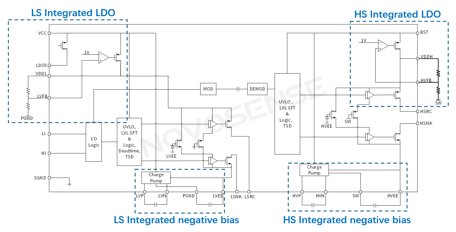
Functional block diagram of NSD2622N
Eliminating false triggering risks and providing more stable drive voltage
Compared to conventional Si MOSFET driver solutions, the key challenge in E-mode GaN driver circuit design lies in providing appropriate, stable and reliable positive/negative bias voltages. This is because that E-mode GaN typically requires a 5V-6V turn-on voltage, while its threshold voltage is as low as 1V, or even lower at high temperatures, necessitating negative turn-off voltage to prevent false triggering. To address this challenge, two common drive solutions are used for E-mode GaN: resistive-capacitive (RC) voltage division drive and direct drive.
1. RC voltage division drive
This approach utilizes standard Si MOSFET driver ICs. As shown in the diagram, during turn-on, the parallel combination of Cc and Ra is connected with Rb in series, dividing the driver supply voltage (e.g., 10V) to provide a 6V gate drive voltage for the GaN device, with Dz1 clamping the positive voltage. During turn-off, Cc discharges to provide negative turn-off voltage for the GaN device, with Dz2 clamping the negative voltage.
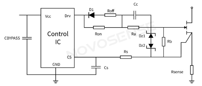
RC voltage division drive solution
Although the RC voltage division circuit does not require sophisticated driver ICs, it introduces additional parasitic inductance due to a large number of components involved, which can impact GaN’s switching performance at high frequencies. Moreover, since the negative turn-off voltage relies on discharge from capacitor Cc, the negative turn-off voltage proves unreliable.
As shown in the half-bridge demo board test waveforms, during the startup phase (T1 in the waveform), the absence of initial charge on Cc results in failure to establish negative voltage and thus zero-voltage turn-off; during the negative turn-off period following the driver’s signal transmission (T2), the negative voltage amplitude fluctuates with capacitor discharge; and during the prolonged turn-off period (T3), the capacitor cannot sustain negative voltage, eventually discharging to zero. Consequently, RC voltage division circuits are generally limited to medium/low power applications with relatively lower reliability requirements, and are proved unsuitable for high-power systems.
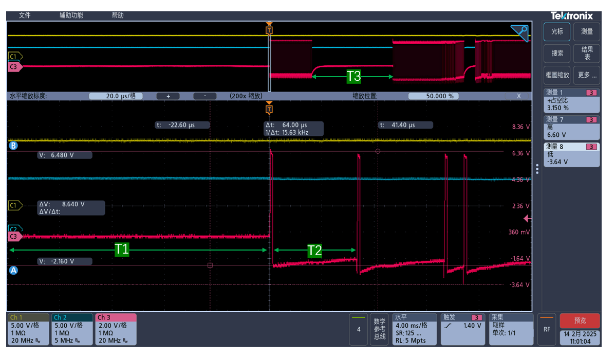
Waveform of E-mode GaN using RC voltage division drive circuit
(CH2: Drive supply voltage; CH3: GaN gate-source voltage)
2. Direct drive
The direct drive solution requires selecting a driver IC with an appropriate undervoltage-lockout (UVLO) threshold, for example, NSI6602VD, which is specifically designed for E-mode GaN with a 4V UVLO threshold. When paired with an external positive/negative voltage regulation circuit, it can directly drive E-mode GaN devices. Below is a typical application circuit.
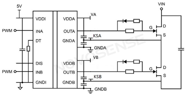
NSI6602VD driver circuit

Positive and negative voltage regulation circuits
This direct drive solution can provide reliable negative turn-off voltage for GaN under all operating conditions, when the auxiliary power supply is functioning normally. As a result, this approach is widely adopted in various high-voltage, high-power GaN applications.
The next-generation GaN driver NSD2622N from NOVOSENSE, integrates the positive/negative voltage regulation circuits directly into the chip. As shown in the half-bridge demo board test waveforms below, NSD2622N maintains consistent negative turn-off voltage amplitude and duration regardless of operating conditions. Specifically, during startup (T1 in the waveform), the negative voltage is established even before the driver sends signals; during GaN turn-off (T2), the negative voltage remains stable in amplitude; during extended periods without driver signals (T3), the negative voltage continues to stay reliably stable.
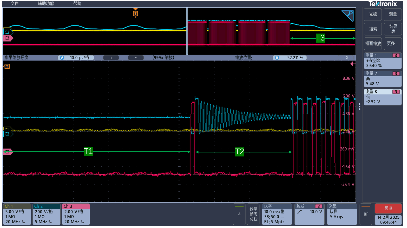
Waveforms of E-mode GaN using NSD2622N driver circuit
(CH2: Low-side GaN Vds, CH3: Low-side GaN Vgs)
Simplified circuit design and reduced system costs
NSD2622N can provide stable and reliable direct drive for GaN devices. More importantly, by integrating positive/negative voltage regulators, it significantly reduces external component count. By adopting the bootstrap supply architecture, NSD2622N greatly simplifies driver power circuit design and lowers overall system costs.
Taking a 3kW power supply unit (PSU) as an example, assuming both phases of the interleaved TTP PFC and full-bridge LLC use GaN devices, a complexity comparison between two direct-drive solutions is given below:
When using the NSI6602VD driver solution, each half-bridge high-side driver requires an independent isolated power supply in conjunction with corresponding isolation and positive/negative voltage regulation circuits. This means complex auxiliary power supply design for isolation. Given the high power quality requirements of GaN driving and the fact that the main power paths of the PFC and LLC stages are typically placed on separate boards, a two-stage auxiliary power architecture is often necessary. In this configuration, the first stage typically employs a device with wide input voltage range like flyback converter, to generate regulated voltage rails. The second stage may use an open-loop full-bridge topology to provide isolated power and further regulate the power to generate the required positive and negative supply voltages for NSI6602VD. Below is a typical power architecture for such a driver solution.
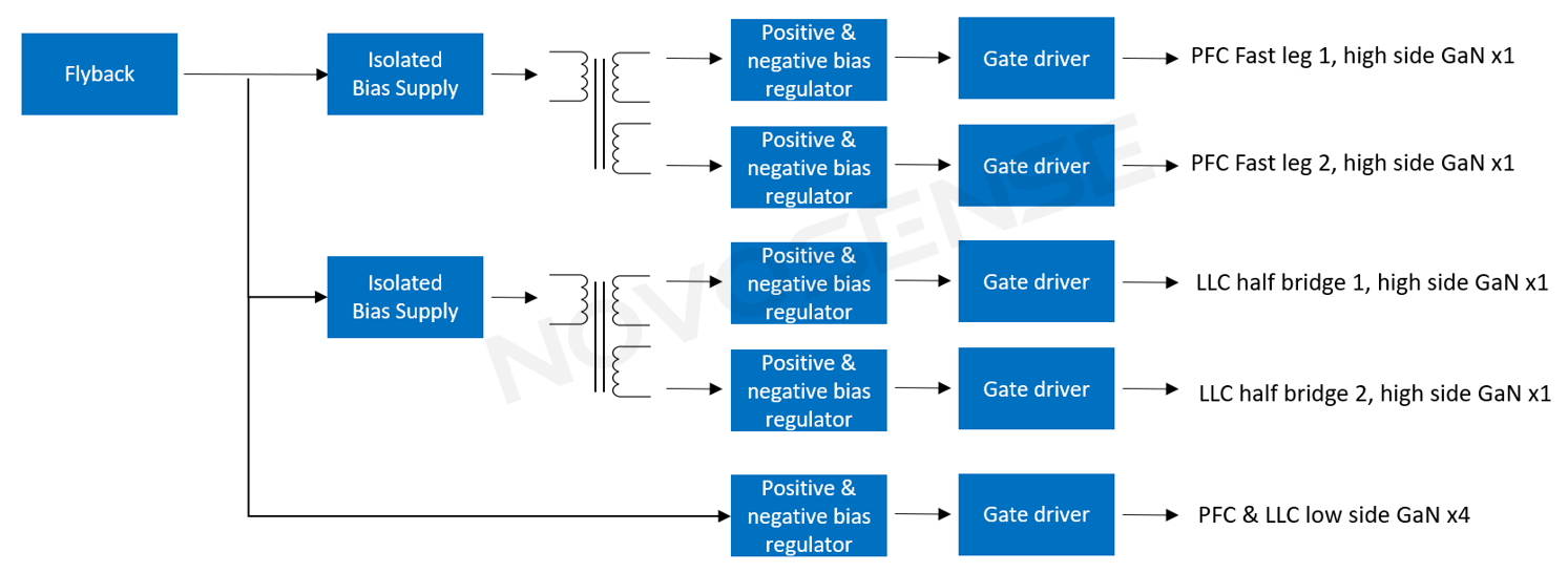
Typical power architecture for NSI6602VD driver solution
The NSD2622N driver solution significantly simplifies auxiliary power design through its bootstrap supply capability. Below is a typical power architecture for this approach.

Typical power architecture for NSD2622N driver solution
A detailed comparison of bill-of-materials (BOM) for driver and power supply circuits between the above-mentioned two GaN direct-drive solutions is provided in the table below. It can be seen that the NSD2622N solution utilizing bootstrap supply, dramatically reduces total component count compared to the NSI6602VD’s isolated power supply approach, resulting in substantially lower system costs. Even in applications requiring isolated power supply, NSD2622N maintains its competitive edge - its integrated positive/negative voltage regulators enable a more simplified peripheral circuit relative to the NSI6602VD solution, leading to fewer components and lower system costs.
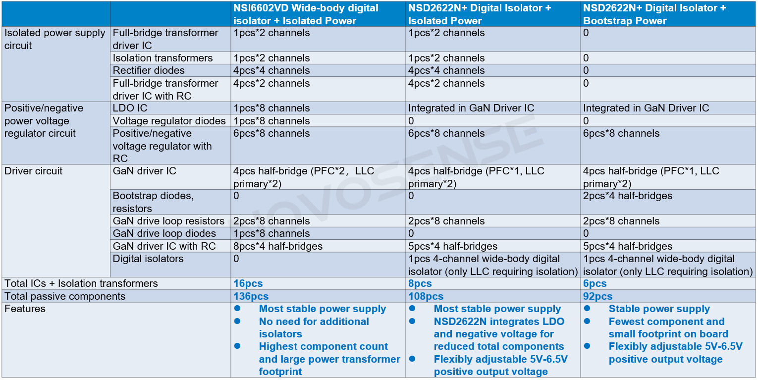
BOM comparison between two GaN direct drive solutions
Versatile GaN compatibility and flexible drive voltage adjustment
The E-mode GaN driver IC NSD2622N from NOVOSENSE delivers not only superior performance but also broad compatibility across various GaN devices from different brands, of different types (including both voltage-mode and current-mode), and at different voltage ratings. For instance, the output voltage of NSD2622N can be set between 5V to 6.5V by adjusting feedback resistors. This enables selection of the most appropriate driving voltage for any GaN device by simply adjusting the feedback resistors to match specific GaN characteristics, allowing GaN devices from different brands to operate at their individual peak performance points.
In addition, NSD2622N features a minimum dv/dt immunity of 200V/ns on the switching node (SW), enhancing the upper limit of GaN switching speed. The adoption of a more compact QFN package and the design of independent turn-on and turn-off output pins further reduce the driver loop parasitic inductance. The over-temperature protection ensures safer GaN applications.
NOVOSENSE also offers single-channel GaN driver IC NSD2012N. Featuring 3mm*3mm QFN package and adjustable negative voltage capability, it can meet more personalized application requirements.
在线留言询价
- 一周热料
- 紧缺物料秒杀
| 型号 | 品牌 | 询价 |
|---|---|---|
| TL431ACLPR | Texas Instruments | |
| MC33074DR2G | onsemi | |
| RB751G-40T2R | ROHM Semiconductor | |
| BD71847AMWV-E2 | ROHM Semiconductor | |
| CDZVT2R20B | ROHM Semiconductor |
| 型号 | 品牌 | 抢购 |
|---|---|---|
| ESR03EZPJ151 | ROHM Semiconductor | |
| STM32F429IGT6 | STMicroelectronics | |
| IPZ40N04S5L4R8ATMA1 | Infineon Technologies | |
| TPS63050YFFR | Texas Instruments | |
| BU33JA2MNVX-CTL | ROHM Semiconductor | |
| BP3621 | ROHM Semiconductor |
- 周排行榜
- 月排行榜
AMEYA360公众号二维码
识别二维码,即可关注


请输入下方图片中的验证码:


