Renesas Electronics IA Functional Safety Reference Board

Release time:2023-03-28
author:AMEYA360
source:网络
reading:6719

  Renesas Electronics IA Functional Safety Reference Board is a solution for ensuring the safety of systems while keeping a tab on development costs. The Renesas Electronics board is based on IEC61508 and meets the HFT=1 and SIL3 requirements. The device is ideal for applications with cost and knowledge limitations for FSoE system development. The board is optimized for BOM cost by integrating EtherCAT and FSoE in one system.
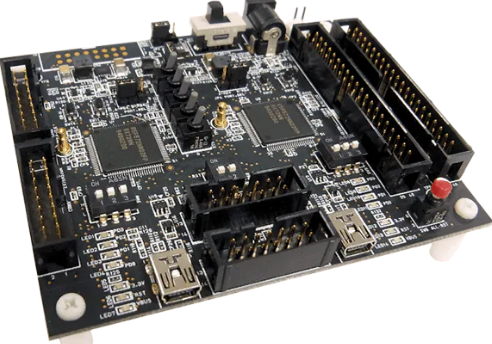
Renesas Electronics IA Functional Safety Reference Board

  FEATURES

  Hardware functionality

  HFT=1, SIL3 architecture

  No external network communication IC is needed

  Coexist w/EtherCAT slave communication by RX72M built-in EtherCAT slave controller (2 ports) and FSoE slave functions

  Safety input five channel

  Safety output eight channel

  Non-safety I/O four channel

  Dual MCU(RX72M+RX23T) configuration board for FSoE Slave function

  Software and documents

  Full set of Renesas’s FuSa SWs

  User manual, schematics, BOM list

  APPLICATIONS

  Safety remote I/O

  Functional safety application for HFT=1 and SIL3 criteria under IEC61508 standards

  AC drive / GP inverter

  Safety system broadly for safety PLC, safety sensors

  Target market segment

  Industrial automation (factory automation, process automation)

  Building automation


("Note: The information presented in this article is gathered from the internet and is provided as a reference for educational purposes. It does not signify the endorsement or standpoint of our website. If you find any content that violates copyright or intellectual property rights, please inform us for prompt removal.")

Previous:

Next:

Online messageinquiry

reading
Renesas Debuts Best-in-Class MCUs Optimized for Single-Motor Applications Including Power Tools, Home Appliances and More
  Renesas Electronics Corporation (TSE:6723), a premier supplier of advanced semiconductor solutions,introduced the RA2T1 microcontroller (MCU) group based on the Arm® Cortex®-M23 processor optimized for motor control systems in July9. RA2T1 devices are specifically designed for single-motor applications such as fans, power tools, vacuum cleaners, refrigerators, printers, hair dryers and many more.  Feature Set Optimized for Motor Control  The new RA2T1 devices include a number of features designed to enhance motor control function, specifically in single-motor systems. One of the notable features is a 3-channel S&H function that simultaneously detects the 3-phase current values of Brushless DC (BLDC) motors. This method provides superior control accuracy as opposed to sequential measurement methods. The RA2T1 MCUs also offer complementary Pulse Width Modulation (PWM) function of the timer, which enables automatic insertion of dead time and generation of an asymmetric PWM. This function is optimized for inverter drive, which facilitates control algorithm implementation.  The RA2T1 devices offer safety features that are critical in motor control applications. They provide a Port Output Enable function and a high-speed comparator that work together to quickly shut off the PWM output when an overcurrent is detected. The shutdown state can be selected according to the inverter specifications.  Renesas Leadership in Embedded Processing for Motor Control  Renesas has shipped motor-control specific MCUs for over 20 years. The company ships over 230 million motor control embedded processors per year to thousands of customers worldwide. In addition to multiple RA MCU groups, Renesas offers motor-control specific devices in its 32-bit RX Family, its 16-bit RL78 MCUs and its 64-bit RZ MPUs.  “Customers have trusted Renesas motor control solutions for many years across thousands of systems,” said Daryl Khoo, Vice President of Embedded Processing Marketing Division at Renesas. “The RA2T1 MCUs enhance our leadership in this area with market-leading technology, low-power operation, and legendary Renesas quality and safety standards for single-motor systems.”  Key Features of the RA2T1 Group MCUs  Core: 64 MHz Arm Cortex-M23  Memory: 64KB Flash, 8KB SRAM, 2KB Data Flash  Analog Peripherals: 12-bit ADC with 3-channel Sample and Hold, temperature sensor, internal reference voltage, 2-channel high-speed comparators  System: High-, mid- and low-speed On-chip Oscillators; clock output; power-on reset; voltage detection; data transfer, event link and interrupt controllers; low-power modes  Safety: PWM forced shutdown, SRAM parity error check, ADC self-diagnosis, clock frequency accuracy measurement, illegal memory access detection  Operating Temperature Range: Ta = -40°C to 125°C  Operating Voltage: 1.6V to 5.5V  Packages: 48LQFP, 32-LQFP, 48-QFN, 32-QFN, 24-QFN (4mm x 4mm)  The new RA2T1 Group MCUs are supported by Renesas’ Flexible Software Package (FSP). The FSP enables faster application development by providing all the infrastructure software needed, including multiple RTOS, BSP, peripheral drivers, middleware, connectivity, networking, and security stacks as well as reference software to build complex AI, motor control and cloud solutions. It allows customers to integrate their own legacy code and choice of RTOS with FSP, thus providing full flexibility in application development. Using the FSP will ease migration of motor control designs to other RA Series devices.  Winning Combinations  Renesas has combined the new RA2T1 Group MCUs with numerous compatible devices from its portfolio to offer a wide array of Winning Combinations, including Portable Power Tools, Smart BLDC Ceiling Fan, Cordless Vacuum Cleaner, Cordless Leaf Blower. Winning Combinations are technically vetted system architectures from mutually compatible devices that work together seamlessly to bring an optimized, low-risk design for faster time to market. Renesas offers more than 400 Winning Combinations with a wide range of products from the Renesas portfolio to enable customers to speed up the design process and bring their products to market more quickly. They can be found at renesas.com/win.  Availability  The RA2T1 Group MCUs are available now, along with the FSP software. The new MCUs are supported in Renesas’ Flexible Motor Control development kit that enables easy evaluation of motor control using permanent magnet synchronous motors (brushless DC motors), and the Renesas Motor Workbench development tool. This development kit offers a common design platform with numerous Renesas motor control MCUs from the RA and RX families, enabling migration of IP across numerous devices. Information on all these offerings is available at renesas.com/RA2T1. Samples and kits can be ordered either on the Renesas website or through distributors.  Renesas MCU Leadership  A world leader in MCUs, Renesas ships more than 3.5 billion units per year, with approximately 50% of shipments serving the automotive industry, and the remainder supporting industrial and Internet of Things applications as well as data center and communications infrastructure. Renesas has the broadest portfolio of 8-, 16- and 32-bit devices, delivering unmatched quality and efficiency with exceptional performance. As a trusted supplier, Renesas has decades of experience designing smart, secure MCUs, backed by a dual-source production model, the industry’s most advanced MCU process technology and a vast network of more than 250 ecosystem partners. For more information about Renesas MCUs, visit renesas.com/MCUs.
2025-07-14 14:38 reading:339
Renesas Strengthens Power Leadership with New GaN FETs for High-Density Power Conversion in AI Data Centers, Industrial and Charging Systems
  Renesas Electronics Corporation (TSE:6723), a premier supplier of advanced semiconductor solutions, introduced three new high-voltage 650V GaN FETs for AI data centers and server power supply systems including the new 800V HVDC architecture, E-mobility charging, UPS battery backup devices, battery energy storage and solar inverters. Designed for multi-kilowatt-class applications, these 4th-generation plus (Gen IV Plus) devices combine high-efficiency GaN technology with a silicon-compatible gate drive input, significantly reducing switching power loss while retaining the operating simplicity of silicon FETs. Offered in TOLT, TO-247 and TOLL package options, the devices give engineers the flexibility to customize their thermal management and board design for specific power architectures.  The new TP65H030G4PRS, TP65H030G4PWS and TP65H030G4PQS devices leverage the robust SuperGaN® platform, a field-proven depletion mode (d-mode) normally-off architecture pioneered by Transphorm, which was acquired by Renesas in June 2024. Based on low-loss d-mode technology, the devices offer superior efficiency over silicon, silicon carbide (SiC), and other GaN offerings. Moreover, they minimize power loss with lower gate charge, output capacitance, crossover loss, and dynamic resistance impact, with a higher 4V threshold voltage, which is not achievable with today’s enhancement mode (e-mode) GaN devices.  Built on a die that is 14 percent smaller than the previous Gen IV platform, the new Gen IV Plus products achieve a lower RDS(on) of 30 milliohms (mΩ), reducing on-resistance by 14 percent and delivering a 20 percent improvement in on-resistance output-capacitance-product figure of merit (FOM). The smaller die size reduces system costs and lowers output capacitance, which results in higher efficiency and power density. These advantages make the Gen IV Plus devices ideal for cost-conscious, thermally demanding applications where high performance, efficiency and small footprint are critical. They are fully compatible with existing designs for easy upgrades, while preserving existing engineering investments.  Available in compact TOLT, TO-247 and TOLL packages, they provide one of the broadest packaging options to accommodate thermal performance and layout optimization for power systems ranging from 1kW to 10kW, and even higher with paralleling. The new surface-mount packages include bottom side (TOLL) and top-side (TOLT) thermal conduction paths for cooler case temperatures, allowing easier device paralleling when higher conduction currents are needed. Further, the commonly used TO-247 package provides customers with higher thermal capability to achieve higher power.  “The rollout of Gen IV Plus GaN devices marks the first major new product milestone since Renesas’ acquisition of Transphorm last year,” said Primit Parikh, Vice President of the GaN Business Division at Renesas. “Future versions will combine the field-proven SuperGaN technology with our drivers and controllers to deliver complete power solutions. Whether used as standalone FETs or integrated into complete system solution designs with Renesas controllers or drivers, these devices will provide a clear path to designing products with higher power density, reduced footprint and better efficiency at a lower total system cost.”  Unique d-mode Normally-off Design for Reliability and Easy Integration  Like previous d-mode GaN products, the new Renesas devices use an integrated low-voltage silicon MOSFET – a unique configuration that achieves seamless normally-off operation while fully capturing the low loss, high efficiency switching benefits of the high- voltage GaN. As they use silicon FETs for the input stage, the SuperGaN FETs are easy to drive with standard off-the-shelf gate drivers rather than specialized drivers that are normally required for e-mode GaN. This compatibility simplifies design and lowers the barrier to GaN adaptation for system developers.  GaN-based switching devices are quickly growing as key technologies for next-generation power semiconductors, fueled by demand from electric vehicles (EVs), inverters, AI data center servers, renewable energy, and industrial power conversion. Compared to SiC and silicon-based semiconductor switching devices, they provide superior efficiency, higher switching frequency and smaller footprints.  Renesas is uniquely positioned in the GaN market with its comprehensive solutions, offering both high- and low-power GaN FETs, unlike many providers whose success in the field has been primarily limited to lower power devices. This diverse portfolio enables Renesas to serve a broader range of applications and customer needs. To date, Renesas has shipped over 20 million GaN devices for high- and low-power applications, representing more than 300 billion hours of field usage.
2025-07-04 15:04 reading:375
Renesas Sets New MCU Performance Bar with 1-GHz RA8P1 Devices with AI Acceleration
Unprecedented 7300+ CoreMarks1 with Dual Arm CPU coresTSMC 22ULL Process Delivers High Performance and Low Power ConsumptionEmbedded MRAM with Faster Write Speeds and Higher Endurance and RetentionDedicated Peripherals Optimized for Vision and Voice AI plus Real-Time AnalyticsNew AI Software Framework Eases Development and Enables Easy Migration with MPUsLeading-Edge Security Features Ensure Data Privacy  Renesas Electronics Corporation (TSE:6723), a premier supplier of advanced semiconductor solutions, introduced the RA8P1 microcontroller (MCU) Group targeted at Artificial Intelligence (AI) and Machine Learning (ML) applications, as well as real-time analytics. The new MCUs establish a new performance level for MCUs by combining 1GHz Arm® Cortex®-M85 and 250MHz Cortex-M33 CPU cores with the Arm Ethos™-U55 Neural Processing Unit (NPU). This combination delivers the highest CPU performance of over 7300 CoreMarks and AI performance of 256 GOPS at 500 MHz.  Designed for Edge/Endpoint AI  The RA8P1 is optimized for edge and endpoint AI applications, using the Ethos-U55 NPU to offload the CPU for compute intensive operations in Convolutional and Recurrent Neural Networks (CNNs and RNNs) to deliver up to 256 MACs per cycle that yield 256 GOPS performance at 500 MHz. The new NPU supports most commonly used networks, including DS-CNN, ResNet, Mobilenet TinyYolo and more. Depending on the neural network used, the Ethos-U55 provides up to 35x more inferences per second than the Cortex-M85 processor on its own.  Advanced Technology  The RA8P1 MCUs are manufactured on the 22ULL (22nm ultra-low leakage) process from TSMC, enabling ultra-high performance with very low power consumption. This process also enables the use of embedded Magnetoresistive RAM (MRAM) in the new MCUs. MRAM offers faster write speeds along with higher endurance and retention compared with Flash.  “There is explosive growth in demand for high-performance edge AIoT applications. We are thrilled to introduce what we believe are the best MCUs to address this trend,” said Daryl Khoo, Vice President of Embedded Processing Marketing Division at Renesas. “The RA8P1 devices showcase our technology and market expertise and highlight the strong partnerships we have built across the industry. Customers are eager to employ these new MCUs in multiple AI applications.”  “The pace of innovation in the age of AI is faster than ever, and new edge use cases demand ever-improving performance and machine learning on-device,” said Paul Williamson, Senior Vice President and General Manager, IoT Line of Business at Arm. “By building on the advanced AI capabilities of the Arm compute platform, Renesas’ RA8P1 MCUs meet the demands of next generation voice and vision applications, helping to scale intelligent, context-aware AI experiences.”  “It is gratifying to see Renesas harness the performance and reliability of TSMC 22ULL embedded MRAM technology to deliver outstanding results for its RA8P1 devices,” said Chien-Hsin Lee, Senior Director of Specialty Technology Business Development at TSMC. “As TSMC continues to advance our embedded non-volatile memory (eNVM) technologies, we look forward to strengthening our long-standing collaboration with Renesas to drive innovation in future groundbreaking devices.”  Robust, Optimized Peripheral Set for AI  Renesas has integrated dedicated peripherals, ample memory and advanced security to address Voice and Vision AI and Real-time Analytics applications. For vision AI, a 16-bit camera interface (CEU) is included that supports sensors up to 5 megapixels, enabling camera and demanding Vision AI applications. A separate MIPI CSI-2 interface offers a low pin-count interface with two lanes, each up to 720Mbps. In addition, multiple audio interfaces including I2S and PDM support microphone inputs for voice AI applications.  The RA8P1 offers both on-chip and external memory options for efficient, low latency neural network processing. The MCU includes 2MB SRAM for storing intermediate activations or graphics framebuffers. 1MB of on-chip MRAM is also available for application code and storage of model weights or graphics assets. High-speed external memory interfaces are available for larger models. SIP options with 4 or 8 MB of external flash in a single package are also available for more demanding AI applications.  New RUHMI Framework  Along with the RA8P1 MCUs, Renesas has introduced RUHMI (Renesas Unified Heterogenous Model Integration), a comprehensive framework for MCUs and MPUs. RUHMI offers efficient AI deployment of the latest neural network models in a framework agnostic manner. It enables model optimization, quantization, graph compilation and conversion, and generates efficient source code. RUHMI provides native support for machine-learning AI frameworks such as TensorFlow Lite, Pytorch & ONNX. It also provides the necessary tools, APIs, code-generator, and runtime needed to deploy a pre-trained neural network, including ready-to-use application examples and models optimized for RA8P1. RUHMI is integrated with Renesas’s own e2Studio IDE to allow seamless AI development. This integration will facilitate a common development platform for MCUs and MPUs.  Advanced Security Features  The RA8P1 MCUs provide leading-edge security for critical applications. The new Renesas Security IP (RSIP-E50D) includes numerous cryptographic accelerators, including CHACHA20, Ed25519, NIST ECC curves up to 521 bits, enhanced RSA up to 4K, SHA2 and SHA3. In concert with Arm TrustZone®, this provides a comprehensive and fully integrated secure element-like functionality. The new MCUs also provides strong hardware Root-of-Trust and Secure Boot with First Stage Bootloader (FSBL) in immutable storage. XSPI interfaces with decryption-on-the-fly (DOTF) allow encrypted code images to be stored in external flash and decrypted on the fly as it is securely transferred to the MCU for execution.  Ready to Use Solutions  Renesas provides a wide range of easy-to-use tools and solutions for the RA8P1 MCUs, including the Flexible Software Package (FSP), evaluation kits and development tools. FreeRTOS and Azure RTOS are supported, as is Zephyr. Several Renesas software example projects and application notes are available to enable faster time to market. In addition, numerous partner solutions are available to support development with the RA8P1 MCUs, including a driver monitoring solution from Nota.AI and a traffic/pedestrian monitoring solution from Irida Labs. Other solutions can be found at the Renesas RA Partner Ecosystem Solutions Page.  Key Features of the RA8P1 MCUs  Processors: 1GHz Arm Cortex-M85, 500MHz Ethos-U55, 250 MHz Arm Cortex-M33 (Optional)  Memory: 1MB/512KB On-chip MRAM, 4MB/8MB External Flash SIP Options, 2MB SRAM fully ECC protected, 32KB I/D caches per core  Graphics Peripherals: Graphics LCD controller supporting resolutions up to WXGA (1280x800), parallel RGB and MIPI-DSI display interfaces, powerful 2D Drawing engine, parallel 16bit CEU and MIPI CSI-2 camera interfaces, 32bit external memory bus (SDRAM and CSC) interface  Other Peripherals: Gigabit Ethernet and TSN Switch, XSPI (Octal SPI) with XIP and DOTF, SPI, I2C/I3C, SDHI, USBFS/HS, CAN-FD, PDM and SSI audio interfaces, 16bit ADC with S/H circuits, DAC, comparators, temperature sensor, timers  Security: Advanced RSIP-E50D cryptographic engine, TrustZone, Immutable storage, secure boot, tamper resistance, DPA/SPA attack protection, secure debug, secure factory programming, Device Lifecycle management  Packages: 224BGA, 289BGA
2025-07-04 14:56 reading:360
Renesas:Enhance HMI User Experience with Built-in Large Memory MPU
  The HMI market continues to drive growth in better user experience and increased automation with the expansion of HMI applications. This results in a strong demand for improved functionality and performance in display-based applications, such as real-time plotting, smooth animation, and USB camera image capture, in affordable systems. Microprocessors (MPUs) with high-speed, large-capacity built-in memory that can be used like microcontrollers (MCUs) are gaining attention in the market. Renesas' RZ/A3M MPU with a built-in 128MB DDR3L SDRAM and a compatible package for a two-layer PCB design is the ideal solution for realizing smooth animation and high-quality HMI at a reasonable system cost.  High-Performance HMI and Real-Time Graphics  Integrating high-speed, large-capacity memory directly into the MPU package offers several advantages, including mitigating concerns about high-speed signal noise on the PCB and simplifying PCB design for the users. The large-capacity memory needed for high-performance HMIs is externally connected to the MPU in the conventional way. Additionally, PCBs equipped with DDR memory and high-speed signal interfaces require multi-layer PCB designs to account for signal noise, making it challenging to reduce PCB costs. Also, the common capacity of on-chip SRAM is typically between 1MB and 10MB, which is too small for high-performance HMIs that need to include a reasonable number of tasks in the near future. To overcome these issues, Renesas released an industry-leading RZ/A3M MPU with a large built-in 128MB DDR3L memory to support high-performance HMI and real-time graphics performance to enhance better and faster user experiences. Most importantly, the board does not require a high-speed signal interface and supports two-layer PCB design to reduce board noise and simplify system development for users.Figure 1. Strengths of Built-in DDR Memory  Designing High-Performance PCBs at a Reasonable System Cost  The number of PCB layers and the ease of design significantly impact the cost of system implementation and maintenance in user applications. As shown in Figure 2, using a wide pin pitch of 0.8mm allows for the layout of signal lines and placement of VIAs between the balls. Additionally, placing the balls handling the main signals in the outer rows of the 244-pin 17mm x 17mm LFBGA package and positioning the GND and power pins as inner balls allows for efficient routing of the necessary signal lines for the system (Figure 3). The RZ/A3M MPU is designed to build cost-effective systems with two-layer PCBs through its innovative packaging and pin assignments.Figure 2. Signal Wiring and Ball LayoutImageFigure 3. Optimized Ball Arrangement for a Two-Layer Board Layout  User-Friendly Interface Enabling Smooth GUI Display  The high-resolution graphic LCD controller integrated into the RZ/A3M supports both parallel RGB and 4-lane MIPI-DSI interfaces, accommodating displays up to 1280x800. Additionally, the 2D graphics engine, high-speed 16-bit 1.6Gbps DDR3L memory, and 1GHz Arm® Cortex®-A55 CPU enable high-performance GUI displays, including smooth animations and real-time plotting that increase the possibility of automation in HMI applications. Connecting a USB camera to the USB 2.0 interface enables smooth capture of camera images, making it easy to check inside of an apparatus, for example, the doneness of the food in the oven or the condition in the refrigerator.  The EK-RZ/A3M is an evaluation kit for the RZ/A3M. It includes an LCD panel with a MIPI-DSI interface. With this kit, users can immediately start evaluation. Renesas also has several graphics ecosystem partners – LVGL, SquareLine Studio, Envox, Crank, RTOSX – who deliver GUI solutions utilizing the EK-RZ/A3M to further accelerate your development cycle.Figure 4. High-Definition HMI Example with the EK-RZ/A3M  The RZ/A3M MPU, equipped with high-speed 128MB DDR3L memory and a 1GHz Arm Cortex-A55, excels in developing cost-effective HMI applications with real-time plot UIs, smooth animations, and USB camera capture. The integrated memory simplifies PCB design by removing the need for high-speed signal interface design. Visit www.renesas.com/rza3m to learn more about the technical details and how to start developing the next HMI applications for consumer electronics, smart home, building automation, healthcare, industrial applications, and office automation.
2025-06-06 15:27 reading:453
  • Week of hot material
  • Material in short supply seckilling
model brand Quote
RB751G-40T2R ROHM Semiconductor
CDZVT2R20B ROHM Semiconductor
BD71847AMWV-E2 ROHM Semiconductor
MC33074DR2G onsemi
TL431ACLPR Texas Instruments
model brand To snap up
ESR03EZPJ151 ROHM Semiconductor
BP3621 ROHM Semiconductor
STM32F429IGT6 STMicroelectronics
TPS63050YFFR Texas Instruments
BU33JA2MNVX-CTL ROHM Semiconductor
IPZ40N04S5L4R8ATMA1 Infineon Technologies
Hot labels
ROHM
IC
Averlogic
Intel
Samsung
IoT
AI
Sensor
Chip
About us

Qr code of ameya360 official account

Identify TWO-DIMENSIONAL code, you can pay attention to

AMEYA360 weixin Service Account AMEYA360 weixin Service Account
AMEYA360 mall (www.ameya360.com) was launched in 2011. Now there are more than 3,500 high-quality suppliers, including 6 million product model data, and more than 1 million component stocks for purchase. Products cover MCU+ memory + power chip +IGBT+MOS tube + op amp + RF Bluetooth + sensor + resistor capacitance inductor + connector and other fields. main business of platform covers spot sales of electronic components, BOM distribution and product supporting materials, providing one-stop purchasing and sales services for our customers.

Please enter the verification code in the image below:

verification code